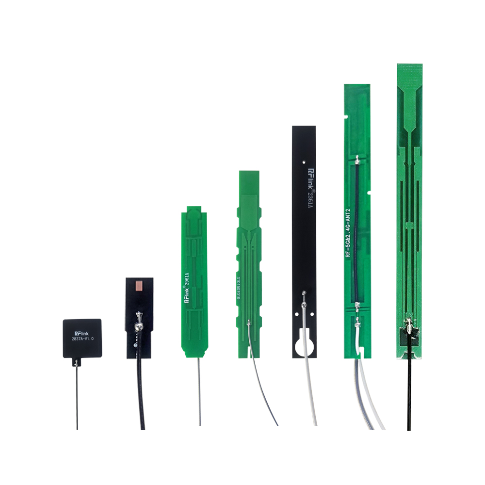
A PCB antenna is a common embedded antenna solution used in compact wireless devices. It is formed by copper traces on a printed circuit board and is widely used in IoT devices, WiFi modules, Bluetooth products, smart meters, remote controls, trackers, and other wireless electronics.
Choosing a PCB antenna is not only about selecting a reference design. The frequency band, PCB size, ground plane, antenna clearance, housing material, nearby components, and matching circuit all affect the final antenna performance.
This guide explains how to choose a PCB antenna for your wireless device and when custom PCB antenna design may be needed.
What Is a PCB Antenna?
A PCB antenna is an antenna structure printed directly on a circuit board. It uses copper traces to radiate and receive RF signals. A PCB antenna can be designed on the main product PCB or on a separate antenna PCB connected to the device.
PCB antennas are popular because they can be compact, cost-effective, and suitable for mass production. They are often used when the product needs an internal antenna without adding an external antenna component.
However, PCB antennas are highly dependent on the product structure. A design that works well on one board may not perform the same way on another device.
When Is a PCB Antenna a Good Choice?
A PCB antenna may be a good choice when:
- The device needs an internal antenna
- The product has enough PCB space
- The housing is mostly plastic
- The antenna can be placed away from metal parts
- Cost control is important for mass production
- The product uses common wireless bands such as WiFi, Bluetooth, Zigbee, LoRa, or sub-GHz
- The design can reserve enough antenna clearance area
For many compact IoT devices, a PCB antenna can provide a good balance between cost, structure, and RF performance.
1. Confirm the Frequency Band
The first step is confirming the operating frequency band. PCB antenna design must match the wireless module and communication standard.
Common PCB antenna frequency bands include:
- 433MHz
- 868MHz
- 915MHz
- 2.4GHz
- 5GHz
- GNSS bands
- LTE or cellular bands in some designs
Lower frequency antennas usually require more physical space because of longer wavelengths. This can make low-frequency PCB antenna design more challenging in compact devices.
A 2.4GHz PCB antenna is usually easier to integrate than a 433MHz PCB antenna because it requires less physical length.
2. Check Available PCB Space
PCB antenna performance depends strongly on available board space. The antenna needs enough physical length and enough clearance from other components.
If the PCB is too small or too crowded, the antenna may have poor efficiency, narrow bandwidth, or unstable performance. This is especially common in compact wireless devices where batteries, displays, sensors, and connectors occupy most of the internal space.
Before choosing a PCB antenna, engineers should evaluate whether the board can provide enough antenna area.
3. Reserve Antenna Clearance
Antenna clearance is one of the most important factors in PCB antenna design. The antenna area should usually be kept away from metal parts, dense copper, batteries, shielding cans, displays, and high-speed circuits.
Poor clearance can cause:
- Lower antenna efficiency
- Detuned frequency response
- Higher VSWR
- Shorter wireless range
- Unstable communication
For this reason, antenna clearance should be considered early in the product design stage. Waiting until the PCB layout is finished may make antenna optimization much harder.
4. Consider the Ground Plane
The ground plane has a strong influence on PCB antenna performance. Many PCB antennas use the ground plane as part of the antenna system. The size, shape, and connection of the ground plane can affect impedance, bandwidth, gain, and radiation pattern.
A larger and well-designed ground plane can often help improve antenna performance. A small or irregular ground plane may limit the antenna’s efficiency and make tuning more difficult.
This is why PCB antenna design should be evaluated together with the whole PCB layout, not only the antenna trace.
5. Evaluate Housing and Nearby Materials
The final device housing can change the antenna performance. Plastic materials, wall thickness, metal parts, screws, batteries, screens, and cables may all affect the antenna.
If a PCB antenna is too close to metal, the signal can be blocked or absorbed. If the housing material has high loss, antenna efficiency may also decrease.
For this reason, PCB antenna testing should be done after the antenna is installed in the actual product structure, not only on an open test board.
6. Check Matching Circuit and VSWR
Most PCB antennas require a matching circuit to improve impedance matching. A matching circuit usually uses components such as capacitors and inductors to tune the antenna for the target frequency band.
VSWR is commonly used to check whether the antenna is properly matched. A lower VSWR usually means less signal reflection. However, VSWR is only one part of antenna performance. Efficiency, gain, radiation pattern, and real communication testing are also important.
7. Standard PCB Antenna or Custom PCB Antenna?
A standard PCB antenna reference design may be useful for some products. However, many real devices require custom PCB antenna design because every product has a different board size, housing, ground plane, component layout, and frequency requirement.
A custom PCB antenna may be needed when:
- The device has limited internal space
- The PCB layout is already fixed
- The ground plane is small or irregular
- The product requires a special frequency band
- Standard antenna performance is unstable after installation
- The antenna must support multiple bands
- The product needs stable performance before certification and mass production
Custom antenna design can help optimize antenna structure, matching circuit, placement, and final performance.
FAQ
What is a PCB antenna?
A PCB antenna is an antenna printed on a circuit board using copper traces to radiate and receive RF signals.
Is a PCB antenna good for compact devices?
Yes, a PCB antenna can be suitable for compact devices, but it requires enough board space, ground plane, and clearance.
Does a PCB antenna need a ground plane?
Many PCB antennas use the ground plane as part of the antenna system, so ground plane design is very important.
Does a PCB antenna need tuning?
Yes. PCB antennas usually need tuning after integration into the final product because the housing, PCB layout, and nearby components can change performance.
Conclusion
Choosing a PCB antenna requires careful evaluation of frequency band, board size, ground plane, antenna clearance, housing material, matching circuit, and final installation conditions.
If a standard PCB antenna cannot meet your requirements for size, frequency, efficiency, VSWR, or product structure, our RF engineering team can help develop and tune a custom PCB antenna solution from design to production.