
An antenna can look excellent on a supplier’s datasheet and still perform poorly after it is installed inside a real product.
The sample may show acceptable VSWR when measured in free space. The radio module may work correctly on an evaluation board. The antenna may even pass a basic bench test before the housing is closed. But after the battery, display, PCB, metal frame, cable, screws, coating, and enclosure are assembled, the resonant frequency may shift, efficiency may fall, and the radiation pattern may change.
This is why antenna selection cannot end with a frequency label and a catalog specification.
For compact IoT devices, smart meters, trackers, security products, gateways, battery systems, remote controls, and connected industrial equipment, the final wireless result depends on the complete device structure. Device-level antenna tuning is the process of evaluating and optimizing the antenna inside the actual product rather than treating it as an isolated component.
This guide explains why antennas detune after integration, how to distinguish detuning from other RF problems, and how to organize a practical tuning and validation process before mass production.
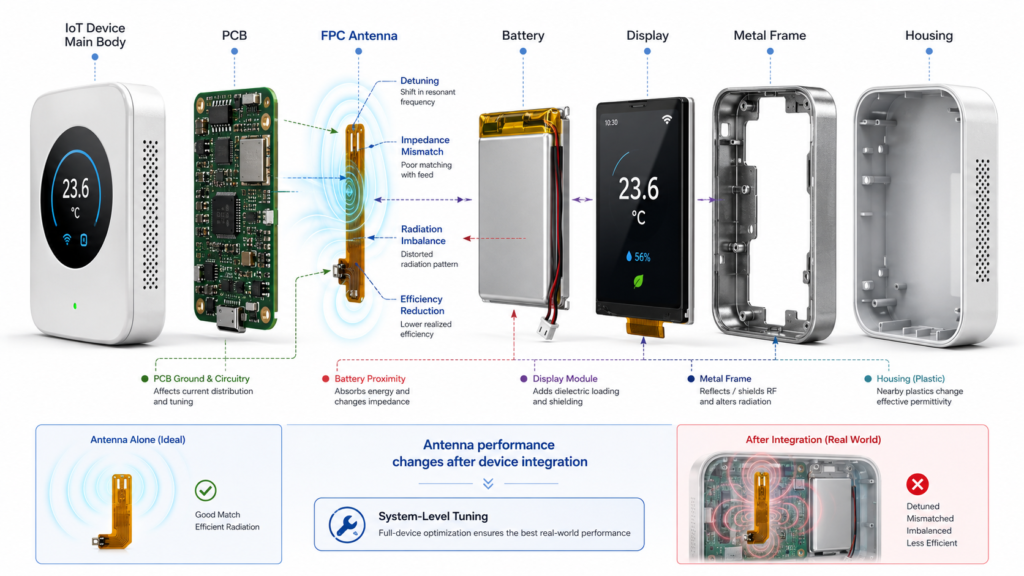
What Does Antenna Detuning Mean?
An antenna is designed to operate over a particular frequency range with a particular impedance, current distribution, and radiation behavior.
When nearby materials or structural changes alter the antenna’s electrical environment, several things may happen:
- The resonant frequency moves higher or lower.
- The impedance at the target frequency changes.
- VSWR or return loss becomes worse.
- Usable bandwidth becomes narrower.
- Radiation efficiency decreases.
- The radiation pattern becomes distorted.
- Polarization behavior changes.
- Performance becomes sensitive to how the user holds or installs the device.
The term “detuning” is often used for all these symptoms, but they are not exactly the same problem.
A resonance shift is primarily a frequency and impedance issue. Low efficiency may result from energy being absorbed or lost near the antenna. Pattern distortion means energy is radiated in different directions than expected. Receiver desensitization may be caused by digital noise or power electronics rather than antenna resonance.
Correct diagnosis matters because changing matching components may help an impedance problem but will not necessarily repair shielding, absorption, noise coupling, or a badly obstructed radiation pattern.
RFLink’s guides to antenna impedance and VSWR explain the relationship between impedance matching, reflected energy, and antenna measurements in more detail.
Why Free-Space Antenna Data Does Not Guarantee Device Performance
Antenna datasheets are useful, but their results normally represent defined test conditions.
Those conditions may use:
- A specified reference ground plane
- A particular evaluation board
- A defined cable length
- A specific antenna orientation
- Open-air or low-obstruction surroundings
- A controlled fixture
- A matching network developed for that reference layout
Your product may use a different PCB size, board stack-up, enclosure, battery, connector, cable route, mounting adhesive, metal structure, or antenna clearance.
For embedded antennas, these differences are part of the antenna system.
A PCB antenna copied from a reference layout may behave differently if the board dimensions change. An FPC antenna may shift after it is attached to a curved plastic surface. A spring antenna may change when a battery or metal bracket is placed beside it. A ceramic antenna may depend strongly on a particular ground-plane size and orientation.
Texas Instruments’ RF Basics guidance notes that nearby metal, plastic enclosures, the human body, PCB layout, and batteries can change antenna impedance and resonant frequency. Nordic Semiconductor’s antenna-interface guidance also emphasizes that matching topology and values must be optimized for the individual antenna application.
The practical lesson is clear: supplier data is a starting point, not a replacement for testing the final assembled device.
1. The PCB and Ground Plane Become Part of the Antenna
For many embedded antenna structures, the visible antenna element is only one part of the radiating system.
The PCB ground plane, return-current path, board dimensions, copper distribution, feed line, and nearby components can contribute significantly to resonance and radiation.
This is particularly important for:
- PCB monopole antennas
- Inverted-F antennas
- Meandered trace antennas
- Ceramic chip antennas
- Spring antennas
- Some FPC antenna installations
Changing the PCB may therefore change the antenna even when the antenna component itself remains unchanged.
PCB Changes That Can Affect Performance
Important variables include:
- Overall PCB length and width
- Ground-plane size and shape
- Layer count and stack-up
- Dielectric thickness
- Copper keep-out area
- Position of ground vias
- Feed-line impedance
- Feed-line length
- Matching-component layout
- Nearby traces and components
- Slots, cut-outs, and board edges
An antenna copied from a reference design should not be assumed to perform identically on a board with different dimensions or materials.
Antenna clearance is also critical. Components, copper, displays, cables, and mechanical structures placed inside the antenna keep-out area can change impedance and reduce efficiency.
RFLink’s PCB antenna selection guide provides additional background on ground planes, antenna clearance, PCB structure, and integration constraints.
2. Batteries Can Shift Resonance and Block Radiation
Batteries are among the most common causes of unexpected antenna changes in compact devices.
They contain conductive materials, occupy a relatively large volume, and are often positioned close to the PCB because product space is limited.
Depending on the antenna structure and battery position, a battery may:
- Couple electrically to the antenna
- Change the effective ground structure
- Shift the resonant frequency
- Absorb or redirect RF energy
- Block radiation in one direction
- Reduce antenna efficiency
- Change performance as the battery position varies during assembly
Coin cells, lithium-polymer pouches, cylindrical cells, and large battery packs create different RF environments.
A battery placed directly under or beside an antenna can be especially problematic. Increasing the separation distance, moving the antenna toward the product edge, changing the antenna orientation, or selecting another antenna type may improve the result.
The battery cable and connector should also be considered. A wire routed through the antenna near field can couple to the antenna and introduce production variation if its route is not controlled.
In sealed battery systems, the problem can become more difficult because the antenna must also work around metal cells, structural frames, waterproofing features, and durable outer housings. RFLink’s smart battery pack antenna case study illustrates why communication, GNSS, sealing, structure, and antenna placement often need to be designed together.
3. Displays, Cameras, Shields, Motors, and Metal Frames Affect the RF Environment
Modern connected devices contain many components that can influence an internal antenna.
Common examples include:
- LCD or OLED display modules
- Display flex cables
- Camera modules
- Speaker magnets
- Motors and gearboxes
- Metal shielding cans
- Heat spreaders
- Structural brackets
- Screws and inserts
- USB or charging connectors
- Large electrolytic components
- Metalized labels or decorative coatings
Metal near an antenna can change current distribution, shift impedance, reflect energy, and block radiation. Even a small screw can matter if it is placed at a sensitive location in the antenna near field.
The effect is not determined only by whether metal exists. Distance, orientation, size, grounding, and location relative to the antenna are all important.
A metal plate behind a directional antenna may be intentional. The same plate placed beside an antenna that was designed for open surroundings may cause serious degradation.
This is why antenna engineers need the real mechanical model, not only a simplified PCB outline.
Late mechanical changes are a frequent source of RF rework. Moving a speaker, adding a metal bracket, changing a camera shield, enlarging a battery, or replacing plastic clips with screws may appear mechanically minor but can require the antenna to be retested.
4. Plastic Enclosures Are Not Electrically Invisible
Plastic does not normally shield RF signals in the same way as a continuous metal enclosure, but it can still affect the antenna.
The influence depends on:
- Plastic type
- Relative permittivity
- Material thickness
- Distance from the antenna
- Curvature
- Moisture absorption
- Fillers and reinforcement materials
- Paint, plating, or decorative coating
- Adhesive tape
- Sealing foam and gaskets
When plastic or adhesive enters the antenna’s near field, it can change the effective electrical length and shift resonance.
An FPC antenna tested while hanging freely may behave differently after it is bonded to a housing wall. Changing the adhesive thickness or moving the FPC closer to the plastic can alter the result.
Glass-filled plastics, carbon-filled materials, metallic paint, vacuum-metallized surfaces, and conductive coatings deserve particular attention because their RF behavior may differ substantially from ordinary unfilled plastic.
The final production material should therefore be used during validation. A 3D-printed prototype made from a different polymer may be useful for mechanical review but may not reproduce the final RF environment accurately.
RFLink’s FPC antenna selection guide explains how installation surface, cable routing, available space, and nearby materials affect flexible antenna integration.
5. Cables and Connectors Can Become Unplanned RF Structures
An FPC cable, coaxial cable, battery wire, display cable, or unshielded harness may interact with the antenna.
The cable may act as:
- Part of the antenna counterpoise
- A parasitic radiating element
- A coupling path to noise
- A path that changes impedance
- An RF current route through the enclosure
- A source of unit-to-unit variation
A coaxial cable does not automatically eliminate these effects. Common-mode current can exist on the cable exterior if the antenna and feed transition are not properly controlled.
Cable routing should therefore be defined rather than left to assembly operators.
Useful controls include:
- Specified cable route
- Defined bend radius
- Fixed attachment points
- Consistent cable length
- Controlled distance from the antenna
- Controlled distance from noisy circuits
- Appropriate connector strain relief
- Repeatable grounding and shielding
A device that passes testing with one carefully arranged prototype cable may fail in production if the cable position varies between units.
Connector choice also matters. An adapter, damaged micro-coax connector, poorly soldered feed point, or loose ground connection can create mismatch and insertion loss that looks like an antenna problem.
6. The User, Mounting Surface, and Installation Environment May Be Part of the Test
A handheld product does not operate only on a laboratory stand.
It may be:
- Held in one or both hands
- Worn on the body
- Mounted on a wall
- Attached to metal equipment
- Installed inside a cabinet
- Placed on concrete
- Fixed to glass
- Positioned beside water
- Mounted in a vehicle
- Installed close to other electronics
The human body can absorb and redirect RF energy, especially when the hand or body is close to the antenna. A device that performs well on a table may change when held normally.
Similarly, a smart meter mounted on a metal panel may behave differently from the same meter tested in open space. A tracker attached to a steel asset may need a different antenna arrangement from a tracker mounted on plastic.
Device-level validation should reproduce the intended use cases.
This may require several test positions:
- Free-standing
- Installed on the target surface
- Held by a user
- Mounted in the normal orientation
- Rotated into likely alternative orientations
- Operated beside typical equipment
- Tested with doors or covers open and closed
The goal is not to optimize every possible position equally. It is to identify the required operating conditions and ensure the antenna has adequate margin in those conditions.
7. Multiple Antennas and Digital Noise Add Another Layer
Many modern devices contain more than one wireless system.
Examples include:
- Cellular and GNSS
- WiFi and Bluetooth
- LoRa and GNSS
- LTE and WiFi
- Bluetooth and NFC
- Multiple cellular antennas
- MIMO antenna systems
These antennas can couple to one another. Their ground structures, feed cables, and radiation patterns may interact.
At the same time, processors, displays, switching regulators, memory buses, USB interfaces, motors, and DC-DC converters can generate noise that reduces receiver sensitivity.
This is an important diagnostic distinction.
A device may show acceptable antenna VSWR but still have poor GNSS reception because digital noise falls inside the GNSS band. A cellular antenna may be matched correctly but have low efficiency because it is blocked by metal. Two antennas may each work separately but perform poorly when both radios operate at the same time.
Testing should therefore include:
- Antenna impedance
- Antenna efficiency
- Radiation pattern
- Isolation between antennas
- Receiver sensitivity or desense
- Simultaneous-radio operation
- Typical processor and display activity
- Charging and motor operating states
Not every wireless problem should be solved by changing the antenna matching circuit.
Detuning, Low Efficiency, Pattern Distortion, or Noise?
The following table helps separate common symptoms.
| Symptom | Possible cause | Useful first check |
|---|---|---|
| Resonance moves outside the target band | Housing, battery, PCB, ground plane, metal or adhesive loading | Measure S11 or VSWR in different assembly states |
| VSWR becomes poor after closing the enclosure | Structural loading, feed issue or matching change | Compare open and closed housing measurements |
| VSWR is acceptable but range remains weak | Low efficiency, pattern blockage, cable loss or receiver noise | Measure efficiency and perform radiated testing |
| Performance is good in one direction but poor in another | Radiation-pattern distortion or shielding | Measure or compare multiple orientations |
| GNSS position is unstable while the antenna match looks normal | Receiver noise, insufficient sky view or active-antenna issue | Check noise spectrum, antenna supply and installed orientation |
| Different production units have different performance | Cable routing, adhesive position, mechanical tolerance or assembly variation | Inspect and measure multiple units |
| Performance drops only when held | Hand or body loading | Repeat tests in representative user positions |
| Performance drops when another radio operates | Antenna coupling or coexistence interference | Measure isolation and simultaneous-radio performance |
A VNA is valuable, but it cannot answer every question in this table.
A Practical Device-Level Antenna Tuning Workflow
A reliable tuning process should begin before the first fully assembled prototype.
Step 1: Define the Wireless Requirements
Document:
- Frequency band or bands
- Target market and regional versions
- Radio technology
- Transmit-power requirements
- Receiver-sensitivity requirements
- Required orientations
- Expected communication environment
- Product dimensions
- Housing materials
- Battery type
- Metal structures
- Required cable and connector
- Number of antennas
- Certification targets
- Production-volume expectations
Avoid using only a vague requirement such as “maximum range.”
A wearable sensor, smart lock, tracking device, industrial gateway, and battery pack may all use the same nominal frequency but require different radiation behavior.
Step 2: Reserve the Antenna Zone Early
The antenna should not be fitted into whatever space remains after the mechanical design is complete.
Reserve:
- Antenna volume
- Keep-out area
- Ground-plane geometry
- Feed-line route
- Matching-network footprint
- Cable route
- Connector access
- Measurement access
- Clearance from batteries and metal
- Space for assembly tolerance
Antenna placement should be reviewed together with the industrial design, PCB design, battery layout, display, and mechanical structure.
Moving the antenna during an early CAD review is much less expensive than redesigning the enclosure after certification testing.
Step 3: Evaluate Candidate Antennas in the Intended Structure
Do not compare antennas only in free space.
Install candidate antennas in a representative device structure using:
- Correct PCB dimensions
- Representative battery
- Intended enclosure material
- Expected cables
- Major metal parts
- Production-like adhesive
- Correct antenna orientation
At this stage, compare not only VSWR but also placement flexibility, assembly repeatability, cable routing, clearance, and likely efficiency.
The smallest antenna is not necessarily the best antenna. A slightly larger antenna with better clearance and repeatability may provide a more reliable production solution.
Step 4: Measure Impedance in Several Assembly States
A useful sequence is:
- Bare PCB
- PCB with antenna
- PCB with battery
- PCB with cables and display
- Open enclosure
- Closed enclosure
- Final screws, seals, labels, and accessories
- Representative mounting or user condition
This sequence shows when the major change occurs.
If resonance shifts when the battery is added, the battery position deserves attention. If the shift appears only after the cover is installed, the housing material, coating, or cover geometry may be responsible.
Measurement setup must also be controlled. The VNA should be calibrated appropriately, and the measurement cable should be positioned consistently so that it does not become an uncontrolled part of the antenna.
Step 5: Tune the Antenna in the Final Representative Device
Matching values should be selected using the actual product environment.
Engineers may adjust:
- Antenna length or geometry
- FPC shape
- Spring dimensions
- Antenna position
- Distance from nearby materials
- Ground clearance
- Feed structure
- Matching capacitors or inductors
- Cable length or route
- Connector location
A configurable matching footprint is useful because it allows different component combinations to be evaluated.
However, matching should not be treated as a substitute for good antenna placement.
Step 6: Measure Efficiency, Gain, and Radiation Pattern
After impedance tuning, perform radiated measurements when the project requires reliable wireless performance.
Useful outputs include:
- Total efficiency
- Radiation efficiency
- Peak gain
- Average gain
- Radiation pattern
- Polarization
- Performance by orientation
- Multi-antenna isolation
RFLink’s article on antenna efficiency explains why good impedance matching alone cannot describe how much input power is actually radiated.
An antenna may show an attractive VSWR curve while surrounding metal or lossy material absorbs much of the energy. This is why efficiency and pattern measurements are important for compact and demanding products.
Step 7: Perform Real Wireless and OTA Tests
The final stage should include the actual radio and software.
Depending on the technology, testing may include:
- Conducted transmit power
- Receiver sensitivity
- Total radiated power
- Total isotropic sensitivity
- Packet delivery
- Throughput
- Connection stability
- GNSS acquisition and tracking
- Different device orientations
- Typical user interaction
- Charging mode
- Display activity
- Motor operation
- Simultaneous-radio operation
Antenna measurements and system measurements should support one another.
An antenna with good chamber results may still be limited by radio configuration or receiver noise. A product with acceptable short-range testing may still lack margin in its real deployment environment.
What a Matching Network Can—and Cannot—Fix
A matching network can transform impedance and reduce reflected power at the target frequency.
It may help correct:
- Moderate resonance shift
- Reactive impedance
- Feed mismatch
- Changes caused by the final enclosure
- Small manufacturing variations
But matching components cannot fully recover energy that is absorbed by nearby lossy materials or blocked by a metal enclosure.
They also cannot automatically correct:
- Severe radiation-pattern obstruction
- An antenna placed inside a closed metal cavity
- Extremely small ground structure
- Strong digital receiver noise
- Poor isolation between antennas
- Damaged cables or connectors
- Incorrect regional frequency selection
- Inconsistent assembly
Matching components also introduce their own loss and tolerance.
The best sequence is therefore:
- Improve placement and clearance.
- Correct the PCB and ground structure.
- Control cables and nearby parts.
- Then optimize the matching network.
- Confirm the result with efficiency and system testing.
A perfect-looking VNA trace can be surprisingly seductive. It is not the whole story.
Choosing Between PCB, FPC, Spring, Ceramic, and External Antennas
| Antenna type | Main integration advantage | Main tuning concern |
|---|---|---|
| PCB trace antenna | Low component cost and repeatable PCB integration | Strong dependence on PCB size, stack-up and ground plane |
| FPC antenna | Flexible placement inside complex housings | Adhesive surface, cable route, bending and nearby materials |
| Spring antenna | Compact three-dimensional structure | Metal clearance, compression, assembly position and ground |
| Ceramic chip antenna | Small standardized component | Reference ground plane, orientation and matching sensitivity |
| Wire antenna | Simple structure and flexible length | Assembly repeatability and uncontrolled routing |
| External antenna | Better separation from internal components | Connector, cable loss, mechanical design and user installation |
The correct choice depends on the complete product.
A PCB antenna may work well when the board dimensions are stable and adequate clearance is available. An FPC antenna can be useful when the housing wall provides a better location than the PCB. A spring antenna can fit compact products but may be sensitive to nearby metal. An external antenna may provide more freedom when internal space or shielding makes embedded performance difficult.
The choice should be made early enough that the enclosure and PCB can support it.
Designing for Production, Not Just One Prototype
A carefully assembled engineering prototype may not represent mass production.
Production variation can come from:
- PCB dielectric tolerance
- Component tolerance
- Antenna dimensional tolerance
- Adhesive placement
- Cable bending
- Connector seating
- Battery movement
- Screw torque
- Plastic material batches
- Coating thickness
- Assembly fixtures
- Alternative approved suppliers
Validation should therefore include multiple units, not only the best-performing prototype.
Useful production controls may include:
- Defined antenna placement drawings
- Cable-routing fixtures
- Adhesive-position marks
- Go/no-go mechanical checks
- VNA or return-loss sampling
- Conducted radio tests
- Golden samples
- Statistical limits
- Change-control requirements
- Retesting after material or supplier changes
The production test does not always need to reproduce the full engineering laboratory evaluation. It should detect the failure modes most likely to occur on the line.
Any change to the antenna, PCB, battery, enclosure material, coating, cable, connector, or major metal part should trigger an RF impact review.
Device-Level Antenna Tuning Checklist
Mechanical Design
- Is the antenna location defined before the enclosure is frozen?
- Is the keep-out area protected?
- Is there adequate clearance from the battery and metal?
- Are production materials represented in prototypes?
- Are screws, coatings, labels, seals, and brackets included?
- Is the antenna protected from movement during assembly?
PCB and RF Path
- Is the PCB stack-up defined?
- Is the ground plane suitable for the antenna type?
- Is the feed line controlled and reasonably short?
- Is a configurable matching footprint available?
- Is there a practical measurement point?
- Are noisy digital signals kept away from the RF path?
Cables and Multiple Antennas
- Is cable routing controlled?
- Are cable length and bend radius specified?
- Is isolation between antennas evaluated?
- Are simultaneous-radio conditions tested?
- Are battery and display cables included in RF validation?
Validation
- Is the antenna measured in the final enclosure?
- Are open and closed housing results compared?
- Are VSWR, efficiency, gain, and pattern considered?
- Is receiver noise checked?
- Are real device orientations tested?
- Are several production-representative units measured?
- Is RF retesting required after structural changes?
FAQ
Why Does an Antenna’s Frequency Shift After It Is Installed?
Nearby plastic, metal, batteries, PCB ground structures, cables, and other materials can change the antenna’s electrical environment and effective electrical length.
The direction and size of the shift depend on the antenna structure and device geometry.
Can Plastic Detune an Antenna?
Yes.
Plastic close to the antenna can change resonance and impedance. The effect depends on the material, thickness, distance, fillers, coatings, adhesive, and antenna type.
Final production materials should be included during validation.
Does a Battery Always Reduce Antenna Performance?
Not always, but batteries frequently affect embedded antennas because of their size, conductive materials, and proximity.
The result may be resonance shift, pattern change, lower efficiency, or a combination of these effects.
Is Good VSWR Enough to Prove the Antenna Works Well?
No.
Good VSWR indicates useful impedance matching, but the antenna may still have low efficiency, an unsuitable radiation pattern, poor isolation, or receiver-noise problems.
Radiated and system-level tests are also necessary.
Can a Matching Circuit Fix Any Detuned Antenna?
No.
A matching circuit can improve impedance, but it cannot fully compensate for severe shielding, absorption, a poor ground structure, digital noise, or an unsuitable antenna position.
When Should Device-Level Antenna Tuning Be Performed?
Initial antenna planning should begin during the early PCB and mechanical design stage.
Final tuning should be performed using a representative assembled device before certification and mass production. RF performance should be reviewed again after significant structural or material changes.
Conclusion
An antenna does not operate independently from the product around it.
The PCB, ground plane, battery, display, metal structure, housing, adhesive, cables, connectors, user, and mounting environment can all influence resonance, impedance, efficiency, and radiation pattern.
A reliable device-level antenna tuning process should therefore:
- Define the real wireless requirements.
- Reserve the antenna area early.
- Evaluate candidates inside the intended structure.
- Measure multiple assembly states.
- Tune using the final representative device.
- Verify efficiency, gain, pattern, and antenna isolation.
- Test the complete radio under realistic operating conditions.
- Validate production variation before release.
RFLink’s custom antenna solutions support requirement review, antenna design, RF simulation, device-level tuning, prototype validation, and production handover for products where standard antennas cannot meet the final structural or performance requirements.
For an initial review, contact RFLink with the target frequency, wireless technology, PCB files, enclosure drawings, battery information, antenna space, materials, cable requirements, regional market, and expected operating conditions.